Nanowires and nanotubes, slender structures that are only a few billionths of a meter in diameter but many thousands or millions of times longer, have become hot materials in recent years. They exist in many forms — made of metals, semiconductors, insulators and organic compounds — and are being studied for use in electronics, energy conversion, optics and chemical sensing, among other fields.
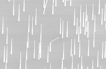
This Scanning Electron Microscope image shows an array of nanowires. (Photo: Kristian Molhave/Opensource Handbook of Nanoscience and Nanotechnology)
The initial discovery of carbon nanotubes — tiny tubes of pure carbon, essentially sheets of graphene rolled up unto a cylinder — is generally credited to a paper published in 1991 by the Japanese physicist Sumio Ijima (although some forms of carbon nanotubes had been observed earlier). Almost immediately, there was an explosion of interest in this exotic form of a commonplace material. Nanowires — solid crystalline fibers, rather than hollow tubes — gained similar prominence a few years later.
Due to their extreme slenderness, both nanotubes and nanowires are essentially one-dimensional. “They are quasi-one-dimensional materials,” says MIT associate professor of materials science and engineering Silvija Gradeèak: “Two of their dimensions are on the nanometer scale.” This one-dimensionality confers distinctive electrical and optical properties.
For one thing, it means that the electrons and photons within these nanowires experience “quantum confinement effects,” Gradeèak says. And yet, unlike other materials that produce such quantum effects, such as quantum dots, nanowires’ length makes it possible for them to connect with other macroscopic devices and the outside world.
The structure of a nanowire is so simple that there’s no room for defects, and electrons pass through unimpeded, Gradeèak explains. This sidesteps a major problem with typical crystalline semiconductors, such as those made from a wafer of silicon: There are always defects in those structures, and those defects interfere with the passage of electrons.
Made of a variety of materials, nanowires can be “grown” on many different substrates through a vapor deposition process. Tiny beads of molten gold or other metals are deposited on a surface; the nanowire material, in vapor, is then absorbed by the molten gold, ultimately growing from the bottom of that bead as a skinny column of the material. By selecting the size of the metal bead, it is possible to precisely control the size of the resulting nanowire.
In addition, materials that don’t ordinarily mix easily can be grown together in nanowire form. For example, layers of silicon and germanium, two widely used semiconductors, “are very difficult to grow together in thin films,” Gradeèak says. “But in nanowires, they can be grown without any problems.” Moreover, the equipment needed for this kind of vapor deposition is widely used in the semiconductor industry, and can easily be adapted for the production of nanowires.
While nanowires’ and nanotubes’ diameters are negligible, their length can extend for hundreds of micrometers, even reaching lengths visible to the unaided eye. No other known material can produce such extreme length-to-diameter ratios: millions of times longer than they are wide.
Because of this, the wires have an extremely high ratio of surface area to volume. That makes them very good as detectors, because all that surface area can be treated to bind with specific chemical or biological molecules. The electrical signal generated by that binding can then easily be transmitted along the wire.
Similarly, nanowires’ shape can be used to produce narrow-beam lasers or light-emitting diodes (LEDs), Gradeèak says. These tiny light sources might someday find applications within photonic chips, for example — chips in which information is carried by light, instead of the electric charges that relay information in today’s electronics.
Compared to solid nanowires, nanotubes have a more complex structure: essentially one-atom-thick sheets of pure carbon, with the atoms arranged in a pattern that resembles chicken wire. They behave in many ways as one-dimensional materials, but are actually hollow tubes, like a long, nanometer-scale drinking straw.
The properties of carbon nanotubes can vary greatly depending on how they are rolled up, a property called chirality. (It’s similar to the difference between forming a paper tube by rolling a sheet of paper lengthwise versus on the diagonal: The different alignments of fibers in the paper produce different strength in the resulting tubes.) In the case of carbon nanotubes, chirality can determine whether the tubes behave as metals or as semiconductors.
But unlike the precise manufacturing control that is possible with nanowires, so far methods for making nanotubes produce a random mix of types, which must be sorted to make use of one particular kind. Besides single-walled nanotubes, they also exist in double-walled and multi-walled forms.
In addition to their useful electronic and optical properties, carbon nanotubes are exceptionally strong, and are used as reinforcing fibers in advanced composite materials. “In any application where one-dimensionality is important, both carbon nanotubes and nanowires would provide benefits,” Gradeèak says.


No comments:
Post a Comment